
Bairou New Materials: A Dark Horse Emerges in the Electronic 3D Printing Track.
February 13, 2026 – According to 3Dzyk, Shenzhen Bairou New Materials Technology Co., Ltd. (“Bairou New Materials”) has recently completed a Series B funding round of 65 million CNY. This round saw continued investment from existing shareholders and the introduction of Suzhou Yunshi Investment. The funds will be primarily used for the construction of a new material manufacturing center, enhancing mass production capabilities for core materials, and the ongoing R&D of related electronic additive manufacturing technologies.
On the surface, this appears to be a routine funding news story. However, viewed against the backdrop of the evolution of electronic manufacturing processes, its significance may extend far beyond that.
When Traditional PCB Begins to “Struggle”
Traditional PCB manufacturing has long relied on wet processes such as electroplating and etching. This system is highly mature, but its drawbacks are becoming increasingly apparent: complex procedures, high usage of chemicals, and mounting environmental pressure. Especially as the layer count of server boards continues to rise and the density of advanced packaging increases, material properties and process windows are approaching their limits.
At this juncture, “electronic additive manufacturing” is no longer just a concept but is beginning to emerge as a new process possibility in electronics manufacturing.
Its Entry Point: Starting with Materials
The emergence of Bairou New Materials arguably came at the right time. However, it differs from overseas companies like Nano Dimension, which are more driven by equipment. Bairou is taking a different path. The former emphasizes complete machine systems and closed printing platforms, while Bairou focuses more on the materials themselves, positioning itself more as a material platform enterprise within the electronic additive manufacturing ecosystem.
Clearly, This Path is Not Easy
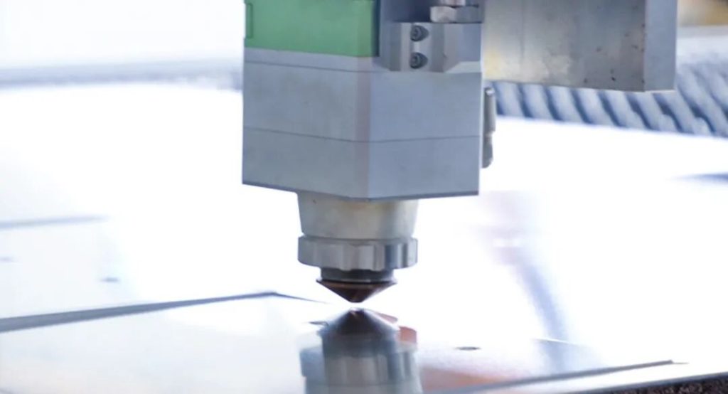
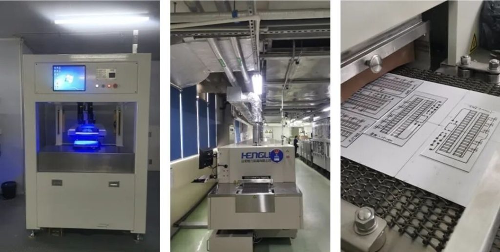
Bairou New Materials’ main technical route starts with nanomaterial preparation, develops functional pastes, adapts to precision inkjet or printing processes, and finally achieves circuit and via formation through low-temperature sintering.
It sounds logical, but anyone who has actually worked with materials knows the significant difficulties involved. Particle size control of nano-metal powders, dispersion stability, sintering window, interfacial bonding strength – every single parameter directly impacts the final reliability.
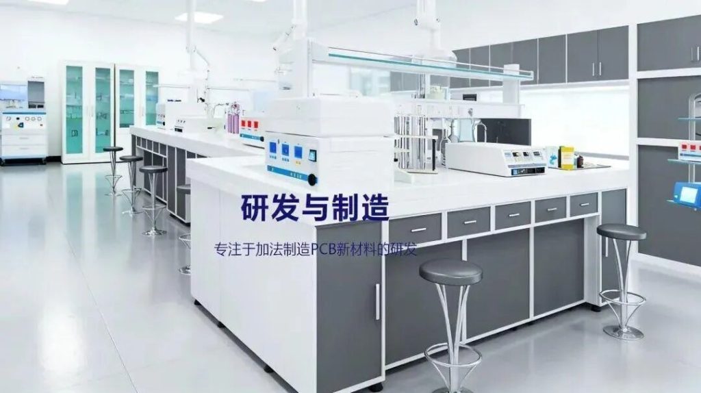
Nine Years to Build a Complete System
After nearly nine years of exploration and adjustment, the company has formed a relatively comprehensive product system in the direction of PCB additive manufacturing, including special via plugging resins, thermally and electrically conductive via plugging copper pastes, nano-sintered conductive interconnection copper pastes, and materials for inkjet-printed circuits and solder masks.
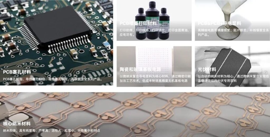
A representative example is its nano-sintered copper paste.
The technical difficulty is there; only certain materials can truly find a balance between “low-temperature sintering” and “high-temperature condition.” For the interlayer interconnection needs of server PCBs with over 70 layers, the nano-copper sintering system indeed provides an alternative path distinct from traditional electroplated copper.
Although it cannot yet vastly replace traditional electroplating on a large scale, it has already gained value worthy of serious evaluation in specific high-end scenarios.
Beyond PCB, Extending into New Energy
In addition to electronic circuit materials, Bairou New Materials is also venturing into lithium battery separator coating materials, including PVDF systems and fluorine-free separator coating powder material CFL, which has already achieved mass production. From a technical logic perspective, this is still an extension of the “materials + precision coating/printing process” approach. Concurrently, the company is exploring the combination of fluorine-free positive electrode binders and solid electrolyte membrane materials with inkjet printing processes.
The Real Test: Scaling Up
Electronic additive manufacturing is still in its early industrial stages, with a long road ahead before reaching scale. This is a fact. The quality of materials isn’t just about lab data; it also depends critically on batch-to-batch stability, consistency in mass production, and cost control.
Following this funding round, Bairou New Materials is accelerating its capacity expansion, including the construction of manufacturing bases in Shenzhen, Dongguan, and a planned site in Huizhou. Transitioning from R&D to large-scale production is a step every materials company must take.
Final Thoughts
To be honest, for a long time in the past, Bairou New Materials had a relatively low profile in the industry, and our attention to it has been limited.
In the past, when mentioning electronic 3D printing, people’s first thought was often Israel’s Nano Dimension. It focused on circuit 3D printing systems, successively acquired Desktop Metal and Markforged, and even attempted to acquire Stratasys, once becoming a focal point in the capital market.
However, looking back over the past couple of years, companies taking different paths have quietly emerged in China. Besides previously reported Xi’an Ruitai Weidong and Beijing Mengzhimo, Bairou New Materials is one of them.
Sometimes, real change in an industry doesn’t necessarily start in the noisiest places.